- Sandisk says 3D Matrix Memory will be an affordable replacement for DRAM
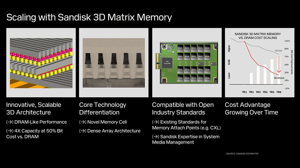
- Will deliver DRAM-like performance at 4x the capacity and half the cost
- Sandisk says it will become more affordable as the technology matures
At its recent Sandisk 2.0 investor day session, the flash storage giant unveiled a series of new SSDs, including a 128TB data center model, while outlining its ambitious roadmap for even larger drives – a 256TB SSD in 2026, a 512TB SSD in 2027, and a whopping 1PB drive expected a few years later.
Sandisk is keen to calm any investor wobbles following its split from Western Digital, and beyond discussing its strategy to boost returns and margins, the company also took the wraps off its groundbreaking 3D Matrix Memory, a scalable memory technology that reportedly promises DRAM-like performance at four times the capacity and half the cost.
Sandisk has positioned 3D Matrix Memory as an affordable solution in response to the end of Moore’s Law for DRAM, where scaling stagnation, a widening compute-memory gap, and soaring memory costs have become major challenges. The company says its scalable memory architecture will break through the “memory wall”, solving the problem of memory capacity and bandwidth struggling to keep pace with ever-increasing processing demands.
More cost-efficient
Developed in collaboration with IMEC, Sandisk’s 3D Matrix Memory is built on a dense array architecture featuring a novel memory cell design while maintaining compatibility with open industry standards, such as CXL.
The company claims its new memory tech will become increasingly more cost-efficient over time. According to a graph Sandisk shared, by Year 6, 3D Matrix Memory will achieve over 50% cost savings per bit compared to DRAM, with a significantly steeper decline in $/GB, making it a more affordable alternative to traditional DRAM solutions.
The company’s development roadmap, shown below, outlines a number of milestones, with transitioning from a 150mm WD Research Fab to a 300mm IMEC Facility in 2024, marking the tech’s first significant step toward large-scale production.
Beginning in 2017, the project has evolved from isolated devices to passive arrays, to CMOS development vehicles. Gen1 media samples will be the next big step and these are expected to reach 32-64Gbit capacities, although there are no details about raw performance, as of yet.